Carrier Board Design – A Step by Step Guide
This presents how to design an M.2 interface and contains a checklist. The integration process is outlined in a step-by-step process.
Step #1: Decide which interfaces to support/implement
There are several interfaces that can be supported. All of them are not always needed. Which ones to support depends on if a general M.2 interface shall be implemented or just for a specific M.2 module. It also depends on if the optional debug interfaces shall be supported.
| Interface | When to implement | Signals |
|---|---|---|
| Powering and enable controls | Always implemented | VBAT (3.3V supply) W_DISABLE1# SUSCLK (32.768kHz clock) |
| Wi-Fi SDIO | Implement if Wi-Fi has SDIO interface | 6 SDIO signals 2 Wi-Fi wakeup signals SDIO_RESET (optional) |
| Wi-Fi PCIe | Implement if Wi-Fi has PCIe interface | 6 PCIe data/clock signals 3 PCIe control signals |
| BT UART | Implement if the Bluetooth interface shall be supported | 4 UART signals W_DISABLE2# 2 Bluetooth wakeup signals |
| BT Audio | Implement if the audio interface of Bluetooth shall be supported | 4 PCM signals |
| Optional | Implement to get a flexible, future-proof M.2 interface | I2C interface, ALARM#, VDDIO voltage override, etc |
| Debug | Implement selected parts of debug interfaces if extra debug support is wanted. Note that all M.2 modules do not support all debug interfaces. Also note that the debug interfaces are not always openly documented. Support from Murata, NXP and/or Cypress is likely to be needed to utilize the features. |
See sections Always Implement to Implement for Bluetooth Audio over PCM for details about the different interfaces. Do not only consider the interfaces needed on the current implementation but also consider future needs. The more of the interfaces and signals that are implemented, the more future-proof the design will be and the easier it will be to change M.2 module in the future.
Step #2: Decide SDIO and interface voltage
The M.2 standard defines two voltage levels that are used, 1.8V (for most data patch signals) and 3.3V (for some control signals).
If compatibility and overall support for most M.2 modules is important, then follow the voltage levels of the M.2 standard. Voltage level shifters will most likely be needed on some of the signals.
If the interface is designed for a specific M.2 module, then there is a feature on some (not all) M.2 modules from Embedded Artists to change the voltage level of the 1.8V level signals to 3.3V signaling level for all signals. Supply a 3.3V voltage to pin 64 on the M.2 connector. Verify with the M.2 module datasheet if this 1.8V VDDIO override is supported, or not.
When 3.3V VDDIO override on 1.8V signals is used, the SDIO voltage level is also changed to 3.3V.
Note that SDIO voltage level is 1.8V, as specified in the M.2 standard. It is not allowed to start at 3.3V and then switch to 1.8V signaling (as is normally done for an SD card interface). The signaling voltage level should be fixed at 1.8V.
Step #3: Design the VBAT power supply
Follow the design recommendations and guidelines outlined in VBAT Power Supply Design Considerations.
Design the power supply with correct tolerance, low-enough voltage ripple, peak current capability and fast transient response.
Always verify the design on prototypes. Measure the different parameters over the full operating temperature range. Measure the step response on current consumption as well as the step response on input voltage variations.
Step #4: Thermal Management
Operating at high ambient temperature, at high data rates and/or at high RF output power levels can generate significant power dissipation from the Wi-Fi/BT chipset on the M.2 module.
Controlling the chipset temperature to within specification is important to sustain the RF performance and lifetime of the components. It is not always possible to dissipate enough heat via natural air convection. By improving thermal dissipation of the Wi-Fi/BT chipset module mounted on the M.2 module, the internal temperature (of the chipset) decreases. This allows the chipset to operate within the RF performance specification and increase the lifetime of the components.
Consult the respective M.2 datasheet for details about operating temperature range. Verify that the surface temperature of the Wi-Fi/BT module on the M.2 board is within specification when operating in the real environment, i.e., inside the enclosure box, transmitting and receiving at the correct data rates.
There are two ways to improve thermal dissipation:
-
Bottom side transfer: Use a thermal pad between the bottom side of the M.2 board and the carrier board PCB (i.e., the PCB under the M.2 board). The thermal pad will transfer the heat from the bottom side of the M.2 module to the carrier board PCB, which should have large copper areas for spreading the transferred heat. For best heat transfer, have gold flashed copper areas with no solder resist on the carrier board PCB.
-
Top side transfer: Transfer the head from the top side of the Wi-Fi/BT module, either directly via a heat sink or via a thermal pad to the enclosure box.
The mechanical enclosure of the system should be designed to allow the heat generated inside the box to be ventilated or spread evenly over the surface areas of the enclosure.
Step #5: Power-up and Power-down Sequences
Follow the design recommendations outlined in Power-up & Reset and Power-down Sequences to implement proper power-up and power-down sequences.
Step #6: Select M.2 connector and stand-off
Embedded Artists use the MDT420E03001 connector from Amphenol, (Digikey part number: MDT420E03001CT-ND, Mouser part number: 523-MDT420E03001). The connector gives 2.54 mm clearance between the bottom side of the mounted M.2 module and the PCB (that the connector is mounted on). There are M.2 connectors with both more and less clearance. If another connector is selected, make sure it is E-key and that the clearance under the mounted M.2 module is sufficient. If no components are mounted under the area that the M.2 module occupies, the clearance can be minimal. Check the M.2 module datasheet for details about bottom side components. For a general design that shall be able to accept all types of M.2 modules (that follow the M.2 standard), make the clearance at least 1.5 mm.
Select a proper standoff for the grounding point in the middle of the M.2 module. The stand-off material shall be metal since it shall be conducting to give a proper grounding point. Note that different M.2 connectors have different heights for the M.2 module over the base PCB. The stand-off must match this height. Embedded Artists use the SM3ZS067U410-NUT1-R1200 stand-off from JAE (Digikey part number: 670-2865-1-ND, Mouser part number: 656-SM3ZS67U41NT1200) and this match the MDT420E03001 connector (2.45 mm high)
Step #7: Create schematic and verify checklist
Create the schematic. Embedded Artists has published schematics for a few different carrier boards that implement the M.2 interface. These schematics can be used as reference when creating the schematic for your specific design. See chapter 6 for details about available design resources.
Use the following checklist to verify that the design is correct. Note that this checklist is not exhaustive and there is no guarantee that the design will work just by following the list, but it will increase the likelihood considerably for success.
Schematic checklist:
- Verify that the schematic symbol for the M.2 connector is correct (pin names and pin numbers).
- Verify that the voltage levels for all signals are correct (1.8V or 3.3V).
- If 3.3V VDDIO override on 1.8V signals is used, verify that the M.2 module support it.
- Verify that the VBAT power supply meets all requirements in Power Supply Design and Management, including power-up and power-down requirements.
- Verify that the 32.678kHz clock signal starts up at least 1 ms before signal W_DISABLE1# is pulled high.
- Verify that the 32.768 kHz clock has 3.3V signaling and a frequency accuracy of ±200 ppm, or better. Verify with M.2 datasheet for details.
- Verify that all power supply and ground pins are connected to the DC supply source, and ground, respectively.
- Add two 100 nF X7R/X5R ceramic capacitors and two >=22uF X7R/X5R ceramic capacitors on VBAT. Voltage rating on the capacitors should be at least 10V. Use good quality components with Equivalent Series Resistance (ESR) not higher than a few milliOhm.
- Do not use ferrite beads for DC filtering of noisy supply voltages.
- If SDIO interface:
- Verify that SDIO voltage is fixed at 1.8V (or 3.3V, if 3.3V VDDIO override is used). This is important also during startup/boot of the system.
- Verify that SDIO_CMD, SDIO_DATA0, SDIO_DATA1, SDIO_DATA2, SDIO_DATA3 all have 10-50K pullup resistors to the supply voltage of SDIO (1.8V, or 3.3V if the VDDIO voltage override feature is used).
- Verify that there is a 10K pullup to 1.8V (or 3.3V, if 3.3V VDDIO override is used) on signal SDIO_WAKE#.
- Place a small, not fitted (i.e., not mounted) capacitor between SDIO_CLK and ground as close as possible to pin 33 of the M.2 connector. This is for EMI debug purpose. A small capacitor (few pF) can be mounted to slow down signal edges (and thereby reducing EMI emission, if needed).
- If PCIe interface:
- Verify that there is a 10K pullup to 3.3V on signal PEWAKE0#, 10K pullup to 3.3V on signal CLKREQ0# and 10K pullup to 3.3V on signal PERST0#.
- Verify that there are 50 ohm parallel termination resistors on the PCIe_CLK signal pair.
- Verify that direction on receive and transmit data pairs is correct.
- If BT interface:
- Verify that there is a 10K pullup to 3.3V on signal UART_WAKE#.
- Verify the directions of the UART signals (RXD connects to TXD and vice versa). As a failsafe, it can be a good idea to add jumpers to be able to switch the signals.
- Verify that the directions of RTS/CTS signals are correct. As a failsafe, it can be a good idea to add jumpers to be able to switch the signals.
- If BT audio interface:
- Verify that the direction of the audio interface signals is correct.
Step #8: Create layout and verify checklist
Create the layout of the schematic. Use the following checklist to verify that the layout is correct. Note that this checklist is not exhaustive and there is no guarantee that the design will work just by following the list, but it will increase the likelihood for success.
Layout checklist:
-
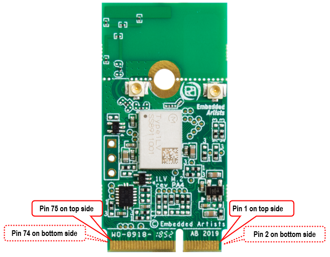
Verify that pin numbering on the M.2 connector is correct, see picture below. A couple of signal groups are marked in the picture and can be used to verify correct pin numbering and orientation of the M.2 connector
-
If SDIO interface:
- Verify that the SDIO signals are routed with correct impedance (50 ohm) over a solid reference plane (GND preferred, but not strictly needed).
- Route the signals so that crosstalk between the SDIO signals and with other signals in the system is minimized. The general method for accomplishing this is have a center-to-center separation between signals of at least 3 times the width of the signal tracks. Even better with 4 times the width. Also avoid running the SDIO bus signals in parallel with other busses for long lengths.
- Verify that all SDIO signals are routed in the same layers, as opposed to for example some signals in layer 1 and some in layer 3. This is to avoid differences in impedance and propagation speed between the signals.
- Verify that the 6 SDIO signals are length matched to 100 mil (if SDIO_CLK is up to 50MHz) or 25 mil (if SDIO_CLK is up to 200MHz). Note that the requirement is not actually length matched signals, but it is a good approximation for time matching of the SDIO signals if the signals as a group are routed through the same layers.
- Keep the SDIO bus to the M.2 connector generally short because it can be a major source of potential EMI issues.
- Verify that there are no stubs on the SDIO signals, for example when connecting the pullup resistors.
-
If PCIe interface:
- Verify that PCIe signals are routed with correct impedance over a solid reference plane (GND preferred, but not strictly needed). PCIe data pairs shall have 85 ohm differential impedance and PCIe clock pair shall have 100 ohm differential impedance.
- Verify that PCIe signals follow general PCIe routing guidelines.
- Verify that the two 50 ohm parallel termination resistors on the PCIe_CLK signal pair are placed close to the M.2 connector. Minimize the stub lengths.
-
Place the VBAT decoupling capacitors close to the M.2 connector.
-
Verify that the grounded stand-off is placed at correct location, see picture above.
-
Verify that clearance under the M.2 module area is enough. Unless absolutely needed, avoid placing components under the area the M.2 module is mounted.
-
If using the on-board PCB trace antenna in the final product, verify that clearance distances are observed. Ideally, arrange the M.2 module so that the antenna is located at a corner of the product. Keep plastic case (i.e., non-metallic) away from the antenna area with at least 5 mm clearance (in all directions). Note that this is a general recommendation - see the specific M.2 module datasheet for details. Also keep any metal elements (e.g., connectors, battery, etc.) away from the antenna area with at least 5 mm clearance (in all directions). Keep a clearance area under and above the antenna area of at least 7.5 mm, both under and over the PCB. Human hands or body parts should be kept away (in the normal use case) from the antenna area.
-
Verify that the layout support thermal management (if that is needed).
Step #9: Verify signal and power quality
Verify the signal and power quality on the prototypes. This section will demonstrate how the SDIO interface can be verified and optimized. The i.MX processors can configure different drive strength on the SDIO interface (and all I/O signals in general). The effect of that is also presented.
First, measuring high speed signals is a challenge. The picture below illustrates SDIO_CLK with a 50MHz clock measures with an active probe having 1.0pF capacitance and 1 GHz bandwidth. The bandwidth of the oscilloscope is 500 MHz.

The picture below illustrates the same SDIO_CLK measures with a passive probe having 11pF capacitance and 500 MHz bandwidth. The signal measured with the active probe is placed in the background as a reference. The signals are relatively similar, but not identical.
")
Below is a 200 MHz SDIO_CLK signals. The orange trace is when measuring with an active probe and the green trance with a passive probe. Here the signals are clearly different and illustrates the importance of measuring high speed signals with a low capacitance probe in order to affect the signal as little as possible.
Also note that the bandwidth of the oscilloscope is 500 MHz, which is too low for measuring a 200 MHz signals with any accuracy. This is also something to consider.
")
The following measurements have been done with an active probe. The picture below illustrates how signal drive strength affects the signal quality. The orange reference trace is the 50 MHz SDIO_CLK seen in the first picture in this section. Drive strength is 75 ohm, medium speed. The yellow trace is when the drive strength is set to 255 ohm, medium speed. Clearly the drive strength is much too low.

The picture below illustrates how it is possible to trim the drive strength, often in small steps. The orange reference trace is the same as before, a 50MHz SDIO_CLK with 75 ohm, medium speed drive strength. The yellow trace is when the drive strength is set to 105 ohm, medium speed. As seen, 75 ohm is clearly better and there is no over/undershoots.

The final picture illustrates when the drive strength is too high. The reference trace is the same as before, a 50MHz SDIO_CLK with 75 ohm, medium speed drive strength. The yellow trace is when the drive strength is set to 40 ohm, max speed. There are clear over/under shoots on the signal which that affect the RF performance of the module.

See the respective M.2 module datasheet for details where to measure the SDIO signals. The signal quality should be verified as close to the Murata module as possible, so the test pads on the M.2 module shall be used. It is not correct to measure for example on the M.2 connector or at the i.MX processor side.
Adjust the SDIO bus drive strength so that signals have clean, defined edges and minimal over/under shoots. Verify that selected settings give reliable performance over the product's temperature range. There is no need to try to create a perfect looking square wave (for the SDIO_CLK signal) because that will generate unnecessary EMC emission.