M.2 Pinning
This chapter presents the pinning used for the M.2 modules from Embedded Artists. It is essentially M.2 Key-E compliant with enhancements to support additional debug signals and 3.3V VDDIO override. The pin assignment for specific control and debug signals has been jointly defined by Embedded Artists, Murata, NXP and Infineon/Cypress.
The Wi-Fi interface is either SDIO, PCIe or USB, depending on the used Murata module.
The Bluetooth interface is UART (and PCM for audio) or USB, depending on the used Murata module.
Optionally, an NFC interface can also be supported via I2C, USB or UART.
Note that the information in the table below is not a complete copy of the M.2 specification. For specific details see the official M.2 specification (PCI Express M.2 Specification), which is available via membership from: www.pcisig.com
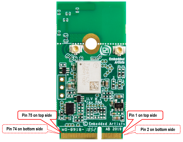
The picture below illustrates the edge pin numbering. It starts on the right edge and alternates between top and bottom side. The removed pads in the keying notch counts (but as obviously non-existing).
The Wi-Fi interface uses either the SDIO, PCIe or the USB interface. The Bluetooth interface typically uses the UART interface for control and PCM interface for audio. The column "When is signal needed" indicates six different categories:
- Always: These signals shall always be connected.
- Wi-Fi SDIO: These signals shall always be connected when the Wi-Fi SDIO interface is used.
- Wi-Fi PCIe: These signals shall always be connected when the Wi-Fi PCIe interface is used.
- Wi-Fi USB: These signals shall always be connected then the Wi-Fi USB interface is used.
- Bluetooth: These signals shall always be connected when the Bluetooth interface is used.
- Bluetooth audio: These signals shall always be connected when the Bluetooth audio interface is used.
- Optional: These signals are optional to connect, e.g., debug interfaces.
The table below lists the pin usage for a general M.2 module with E-keying and SDIO, PCIe or USB interface. Note that all M.2 modules do not support all features and do not connect all pins. See the specific M.2 module datasheet for details.
Note that the M.2 standard defines different voltage levels on different pins. Both 1.8V and 3.3V signaling is used.
| Pin # | Side of pcb | M.2 Name | Voltage Level and Signal Direction | When is signal needed | Note |
|---|---|---|---|---|---|
| 1 | Top | GND | GND | Always | Connect to ground |
| 2 | Bottom | 3.3 V | Always | Power supply input. Connect to stable, low-noise 3.3V supply. Current consumption depends on used M.2 module. Up to 3A might be needed for some MIMO Wi-Fi modules. | |
| 3 | Top | USB_D+ | - | Wi-Fi USB | Connected to USB interface of the module if it exists. |
| 4 | Bottom | 3.3 V | Always | Power supply input. Connect to stable, low-noise 3.3V supply. Current consumption depends on used M.2 module. Up to 3A might be needed for some MIMO Wi-Fi modules. | |
| 5 | Top | USB_D- | Wi-Fi USB | Connected to USB interface of the module if it exists. | |
| 6 | Bottom | LED_1# | OD output from M.2 | Currently not used but can be in the future. | |
| 7 | Top | GND | GND | Always | Connect to ground |
| 8 | Bottom | PCM_CLK | 1.8V I/O | Bluetooth audio | For Bluetooth audio interface: BT_PCM_CLK |
| 9 | Top | SDIO CLK | 1.8V Input to M.2 | Wi-Fi SDIO | For Wi-Fi SDIO interface: SDIO_CLK |
| 10 | Bottom | PCM_SYNC | 1.8V I/O | Bluetooth audio | For Bluetooth audio interface: BT_PCM_SYNC |
| 11 | Top | SDIO CMD | 1.8V I/O | Wi-Fi SDIO | For Wi-Fi SDIO interface: SDIO_CMD Note: Require an external 10-50K ohm pullup |
| 12 | Bottom | PCM_OUT | 1.8V output from M.2 | Bluetooth audio | For Bluetooth audio interface: BT_PCM_OUT |
| 13 | Top | SDIO DATA0 | 1.8V I/O | Wi-Fi SDIO | For Wi-Fi SDIO interface: SDIO_D0 Note: Require an external 10-50K ohm pullup |
| 14 | Bottom | PCM_IN | 1.8V input to M.2 | Bluetooth audio | For Bluetooth audio interface: BT_PCM_IN |
| 15 | Top | SDIO DATA1 | 1.8V I/O | Wi-Fi SDIO | For Wi-Fi SDIO interface: SDIO_D1 Note: Require an external 10-50K ohm pullup |
| 16 | Bottom | LED_2# | OD output from M.2 | Currently not used but can be in the future. | |
| 17 | Top | SDIO DATA2 | 1.8V I/O | Wi-Fi SDIO | For Wi-Fi SDIO interface: SDIO_D2 Note: Require an external 10-50K ohm pullup |
| 18 | Bottom | GND | Always | Connect to ground | |
| 19 | Top | SDIO DATA3 | 1.8V I/O | Wi-Fi SDIO | For Wi-Fi SDIO interface: SDIO_D3 Note: Require an external 10-50K ohm pullup |
| 20 | Bottom | UART WAKE# | 3.3V OD output from M.2 | Bluetooth | For Bluetooth UART interface: Signal from Bluetooth function to wake the host processor. Active low, i.e., wake when signal is low. Named BT_HOST_WAKE_L or BT_WAKE_OUT, depending on wireless chipset. Require an external 10K pullup resistor to 3.3V. |
| 21 | Top | SDIO WAKE# | 1.8V OD output from M.2 | Wi-Fi SDIO | For Wi-Fi SDIO interface: Signal from Wi-Fi function to wake the host processor. Active low, i.e., wake when signal is low. Named WL_HOST_WAKE_L or WL_WAKE_OUT, depending on wireless chipset. Require an external 10K pullup resistor to 1.8V. |
| 22 | Bottom | UART TXD | 1.8V output from M.2 | Bluetooth | For Bluetooth UART interface: BT_UART_TXD Connect to UART_RXD on target processor. |
| 23 | Top | SDIO RESET# | 1.8V input to M.2 | Optional | For Wi-Fi SDIO interface: optional, independent reset of Wi-Fi interface. Active low. Note that this is an optional signal is not used on all M.2 modules. Pin 56 (W_DISABLE1#) is often used to control the Wi-Fi interface but sometimes it controls all of the module, as a general power down signal, and then pin 23 (SDIO RESET#) is used for individual control of the Wi-Fi functionality. |
| 24 | Key, non-existing | ||||
| 25 | Key, non-existing | ||||
| 26 | Key, non-existing | ||||
| 27 | Key, non-existing | ||||
| 28 | Key, non-existing | ||||
| 29 | Key, non-existing | ||||
| 30 | Key, non-existing | ||||
| 31 | Key, non-existing | ||||
| 32 | Bottom | UART_RXD | 1.8V input to M.2 | Bluetooth | For Bluetooth UART interface: BT_UART_RXD Connect to UART_TXD on target processor. |
| 33 | Top | GND | Always | Connect to ground | |
| 34 | Bottom | UART_RTS | 1.8V output from M.2 | Bluetooth | For Bluetooth UART interface: BT_UART_RTS Connect to UART_CTS on target processor and verify that this pin is actually an input on the target processor. |
| 35 | Top | PERp0 | PCIe data input to M.2 | Wi-Fi PCIe | For Wi-Fi PCIe interface: transmit data from host processor |
| 36 | Bottom | UART_CTS | 1.8V input to M.2 | Bluetooth | For Bluetooth UART interface: BT_UART_CTS Connect to UART_RTS on target processor and verify that this pin is actually an output on the target processor. |
| 37 | Top | PERn0 | PCIe data input to M.2 | Wi-Fi PCIe | For Wi-Fi PCIe interface: transmit data from host processor |
| 38 | Bottom | VENDOR DEFINED | 1.8V I/O | Optional | If possible, the JTAG_TDO signal is connected to this pin |
| 39 | Top | GND | Always | Connect to ground | |
| 40 | Bottom | VENDOR DEFINED | 1.8V input to M.2 | Wi-Fi SDIO | For Wi-Fi SDIO interface: Signal from host processor to wake the Wi-Fi functionality. Active low, i.e., wake when signal is low. Named WL_DEV_WAKE_L or WL_WAKE_IN, depending on wireless chipset. |
| 41 | Top | PETp0 | PCIe data output from M.2 | Wi-Fi PCIe | For Wi-Fi PCIe interface: receive data to host processor |
| 42 | Bottom | VENDOR DEFINED | 1.8V input to M.2 | Bluetooth | For Bluetooth UART interface: Signal from host processor to wake the Bluetooth functionality. Active low, i.e., wake when signal is low. Named BT_DEV_WAKE_L or BT_WAKE_IN, depending on wireless chipset. |
| 43 | Top | PETn0 | PCIe data output from M.2 | Wi-Fi PCIe | For Wi-Fi PCIe interface: receive data to host processor |
| 44 | Bottom | COEX3 | 1.8V I/O | Optional | If possible, the JTAG_TDI signal is connected to this pin |
| 45 | Top | GND | Always | Connect to ground | |
| 46 | Bottom | COEX_TXD | 1.8V I/O | Optional | If possible, the JTAG_TCK signal is connected to this pin |
| 47 | Top | REFCLKp0 | PCIe clock input to M.2 | Wi-Fi PCIe | For Wi-Fi PCIe interface: 100MHz reference clock input |
| 48 | Bottom | COEX_RXD | 1.8V I/O | Optional | If possible, the JTAG_TMS signal is connected to this pin |
| 49 | Top | REFCLKn0 | PCIe clock input to M.2 | Wi-Fi PCIe | For Wi-Fi PCIe interface: 100MHz reference clock input |
| 50 | Bottom | SUSCLK | 3.3V input to M.2 | Always | External sleep clock input (32.768kHz) |
| 51 | Top | GND | Always | Connect to ground | |
| 52 | Bottom | PERST0# | 3.3V input to M.2 | Wi-Fi PCIe | For Wi-Fi PCIe interface: Reset input signal, active low. |
| 53 | Top | CLKREQ0# | 3.3V OD output from M.2 | Wi-Fi PCIe | For Wi-Fi PCIe interface: Clock request output from M.2 Require an external 10K pullup resistor to 3.3V. |
| 54 | Bottom | W_DISABLE2# | 3.3V input to M.2 | Bluetooth | Independent software reset of the Bluetooth functionality. This signal is sometimes called BT_REG_ON. A high signal = Bluetooth enabled, a low signal = disabled. |
| 55 | Top | PEWAKE0# | 3.3V input to M.2 | Wi-Fi PCIe | For Wi-Fi PCIe interface: Wakeup request from M.2 Require an external 10K pullup resistor to 3.3V. |
| 56 | Bottom | W_DISABLE1# | 3.3V input to M.2 | Always | Full power control over module or independent software reset of the Wi-Fi functionality. This signal is sometimes called WL_REG_ON. Some wireless chipsets have one common power control signal and then this signal controls the full power of the module, while some chipsets have independent Wi-Fi and Bluetooth power control and then this signal controls the Wi-Fi functionality of the module. A high signal = Module/Wi-Fi enabled, a low signal = disabled. |
| 57 | Top | GND | Always | Connect to ground | |
| 58 | Bottom | I2C_SDA | 1.8V I/O | I2C interface, data signal. According to standard I2C interface implementation, this signal requires an external pullup resistor to 1.8V. Exact value depends on implementation. 1.5K-4.7K ohm is a common value. | |
| 59 | Top | Reserved | 1.8V I/O | ||
| 60 | Bottom | I2C_CLK | 1.8V input to M.2 | I2C interface, clock signal. According to standard I2C interface implementation, this signal requires an external pullup resistor to 1.8V. Exact value depends on implementation. 1.5K-4.7K ohm is a common value. | |
| 61 | Top | Reserved | 1.8V I/O | ||
| 62 | Bottom | ALERT# | 1.8V OD output from M.2 | Optional | Optional interrupt signal from wireless chipset. Require an external 10K pullup resistor to 1.8V. |
| 63 | Top | GND | Always | Connect to ground | |
| 64 | Bottom | RESERVED | On some M.2 modules from Embedded Artists, it is possible to apply a stable, low-noise, 3.3V / 100mA supply to this signal in order to get 3.3V voltage level on all signals. Note that this is a nonfunction is non-standard, i.e., not part of the M.2 specification. | ||
| 65 | Top | Reserved | 1.8V output from M.2 | ||
| 66 | Bottom | UIM_SWP | 1.8V I/O | Optional | In a previous pinning definition, this pin was defined as a signal from host processor to wake the Wi-Fi functionality. Active low, i.e., wake when signal is low. Note that this functionality has moved to pin 40 instead. |
| 67 | Top | Reserved | 1.8V input to M.2 | Optional | |
| 68 | Bottom | UIM_POWER_SNK | 1.8V I/O | ||
| 69 | Top | GND | Always | Connect to ground | |
| 70 | Bottom | UIM_POWER_SRC/GPIO_1 | 1.8V I/O | ||
| 71 | Top | Reserved | 1.8V I/O | ||
| 72 | Bottom | 3.3 V | Always | Power supply input. Connect to stable, low-noise 3.3V supply. Current consumption depends on used M.2 module. Up to 3A might be needed for some MIMO Wi-Fi modules. | |
| 73 | Top | Reserved | 1.8V I/O | ||
| 74 | Bottom | 3.3 V | Always | Power supply input. Connect to stable, low-noise 3.3V supply. Current consumption depends on used M.2 module. Up to 3A might be needed for some MIMO Wi-Fi modules. | |
| 75 | Top | GND | Always | Connect to ground |
It can be difficult to get an overview of the table above. The tables below list the needed signals to implement based on which interfaces to implement.
Always Implement
The signals below should always be implemented/connected.
| Pin # | Side of pcb | M.2 Name | Voltage Level and Signal Direction | When is signal needed | Note |
|---|---|---|---|---|---|
| 1 | Top | GND | GND | Always | Connect to ground |
| 2 | Bottom | 3.3 V | Always | Power supply input. Connect to stable, low-noise 3.3V supply. Current consumption depends on used M.2 module. Up to 3A might be needed for some MIMO Wi-Fi modules. | |
| 4 | Bottom | 3.3 V | Always | Power supply input. Connect to stable, low-noise 3.3V supply. Current consumption depends on used M.2 module. Up to 3A might be needed for some MIMO Wi-Fi modules. | |
| 7 | Top | GND | GND | Always | Connect to ground |
| 18 | Bottom | GND | Always | Connect to ground | |
| 33 | Top | GND | Always | Connect to ground | |
| 39 | Top | GND | Always | Connect to ground | |
| 45 | Top | GND | Always | Connect to ground | |
| 50 | Bottom | SUSCLK | 3.3V input to M.2 | Always | External sleep clock input (32.768kHz) that is used for low-power mode timing on many M.2 modules. Leave open or ground if no clock signal is provided. |
| 51 | Top | GND | Always | Connect to ground | |
| 56 | Bottom | W_DISABLE1# | 3.3V input to M.2 | Always | Full power control over module or independent software reset of the Wi-Fi functionality. This signal is sometimes called WL_REG_ON. Some wireless chipsets have one common power control signal and then this signal controls the full power of the module, while some chipsets have independent Wi-Fi and Bluetooth power control and then this signal controls the Wi-Fi functionality of the module. A high signal = Module/Wi-Fi enabled, a low signal = disabled. |
| 57 | Top | GND | Always | Connect to ground | |
| 63 | Top | GND | Always | Connect to ground | |
| 69 | Top | GND | Always | Connect to ground | |
| 72 | Bottom | 3.3 V | Always | Power supply input. Connect to stable, low-noise 3.3V supply. Current consumption depends on used M.2 module. Up to 3A might be needed for some MIMO Wi-Fi modules. | |
| 74 | Bottom | 3.3 V | Always | Power supply input. Connect to stable, low-noise 3.3V supply. Current consumption depends on used M.2 module. Up to 3A might be needed for some MIMO Wi-Fi modules. | |
| 75 | Top | GND | Always | Connect to ground |
Implement for Wi-Fi over SDIO
The signals below should always be implemented/connected to support Wi-Fi over SDIO
| Pin # | Side of pcb | M.2 Name | Voltage Level and Signal Direction | When is signal needed | Note |
|---|---|---|---|---|---|
| 9 | Top | SDIO CLK | 1.8V Input to M.2 | Wi-Fi SDIO | For Wi-Fi SDIO interface: SDIO_CLK |
| 11 | Top | SDIO CMD | 1.8V I/O | Wi-Fi SDIO | For Wi-Fi SDIO interface: SDIO_CMD Note: Require an external 10-50K ohm pullup |
| 13 | Top | SDIO DATA0 | 1.8V I/O | Wi-Fi SDIO | For Wi-Fi SDIO interface: SDIO_D0 Note: Require an external 10-50K ohm pullup |
| 15 | Top | SDIO DATA1 | 1.8V I/O | Wi-Fi SDIO | For Wi-Fi SDIO interface: SDIO_D1 Note: Require an external 10-50K ohm pullup |
| 17 | Top | SDIO DATA2 | 1.8V I/O | Wi-Fi SDIO | For Wi-Fi SDIO interface: SDIO_D2 Note: Require an external 10-50K ohm pullup |
| 19 | Top | SDIO DATA3 | 1.8V I/O | Wi-Fi SDIO | For Wi-Fi SDIO interface: SDIO_D3 Note: Require an external 10-50K ohm pullup |
| 21 | Top | SDIO WAKE# | 1.8V OD output from M.2 | Wi-Fi SDIO | For Wi-Fi SDIO interface: Signal from Wi-Fi function to wake the host processor. Active low, i.e., wake when signal is low. Named WL_HOST_WAKE_L or WL_WAKE_OUT, depending on wireless chipset. Require an external 10K pullup resistor to 1.8V. |
| 23 | Top | SDIO RESET# | 1.8V input to M.2 | Optional | For Wi-Fi SDIO interface: optional, independent reset of Wi-Fi interface. Active low. Note that this is an optional signal is not used on all M.2 modules. Pin 56 (W_DISABLE1#) is often used to control the Wi-Fi interface but sometimes it controls all of the module, as a general power down signal, and then pin 23 (SDIO RESET#) is used for individual control of the Wi-Fi functionality. |
| 40 | Bottom | VENDOR DEFINED | 1.8V input to M.2 | Wi-Fi SDIO | For Wi-Fi SDIO interface: Signal from host processor to wake the Wi-Fi functionality. Active low, i.e., wake when signal is low. Named WL_DEV_WAKE_L or WL_WAKE_IN, depending on wireless chipset. |
Implement for Wi-Fi over PCIe
The signals below should always be implemented/connected to support Wi-Fi over PCIe
| Pin # | Side of pcb | M.2 Name | Voltage Level and Signal Direction | When is signal needed | Note |
|---|---|---|---|---|---|
| 35 | Top | PERp0 | PCIe data input to M.2 | Wi-Fi PCIe | For Wi-Fi PCIe interface: transmit data from host processor |
| 37 | Top | PERn0 | PCIe data input to M.2 | Wi-Fi PCIe | For Wi-Fi PCIe interface: transmit data from host processor |
| 41 | Top | PETp0 | PCIe data output from M.2 | Wi-Fi PCIe | For Wi-Fi PCIe interface: receive data to host processor |
| 43 | Top | PETn0 | PCIe data output from M.2 | Wi-Fi PCIe | For Wi-Fi PCIe interface: receive data to host processor |
| 47 | Top | REFCLKp0 | PCIe clock input to M.2 | Wi-Fi PCIe | For Wi-Fi PCIe interface: 100MHz reference clock input |
| 49 | Top | REFCLKn0 | PCIe clock input to M.2 | Wi-Fi PCIe | For Wi-Fi PCIe interface: 100MHz reference clock input |
| 52 | Bottom | PERST0# | 3.3V input to M.2 | Wi-Fi PCIe | For Wi-Fi PCIe interface: Reset input signal, active low. |
| 53 | Top | CLKREQ0# | 3.3V OD output from M.2 | Wi-Fi PCIe | For Wi-Fi PCIe interface: Clock request output from M.2 Require an external 10K pullup resistor to 3.3V. |
| 55 | Top | PEWAKE0# | 3.3V input to M.2 | Wi-Fi PCIe | For Wi-Fi PCIe interface: Wakeup request from M.2 Require an external 10K pullup resistor to 3.3V. |
Implement for Wi-Fi and/or Bluetooth over USB
The signals below should always be implemented/connected to support Wi-Fi and/or Bluetooth over USB.
| Pin # | Side of pcb | M.2 Name | Voltage Level and Signal Direction | When is signal needed | Note |
|---|---|---|---|---|---|
| 3 | Top | USB_D+ | - | Wi-Fi USB | Connected to USB interface of the module if it exists. |
| 5 | Top | USB_D- | Wi-Fi USB | Connected to USB interface of the module if it exists. |
Implement for Bluetooth over UART
The signals below should always be implemented/connected to support Bluetooth over UART.
| Pin # | Side of pcb | M.2 Name | Voltage Level and Signal Direction | When is signal needed | Note |
|---|---|---|---|---|---|
| 20 | Bottom | UART WAKE# | 3.3V OD output from M.2 | Bluetooth | For Bluetooth UART interface: Signal from Bluetooth function to wake the host processor. Active low, i.e., wake when signal is low. Named BT_HOST_WAKE_L or BT_WAKE_OUT, depending on wireless chipset. Require an external 10K pullup resistor to 3.3V. |
| 22 | Bottom | UART_TXD | 1.8V output from M.2 | Bluetooth | For Bluetooth UART interface: BT_UART_TXD Connect to UART_RXD on target processor. |
| 32 | Bottom | UART_RXD | 1.8V input to M.2 | Bluetooth | For Bluetooth UART interface: BT_UART_RXD Connect to UART_TXD on target processor. |
| 34 | Bottom | UART_RTS | 1.8V output from M.2 | Bluetooth | For Bluetooth UART interface: BT_UART_RTS Connect to UART_CTS on target processor and verify that this pin is actually an input on the target processor. |
| 36 | Bottom | UART_CTS | 1.8V input to M.2 | Bluetooth | For Bluetooth UART interface: BT_UART_CTS Connect to UART_RTS on target processor and verify that this pin is actually an output on the target processor. |
| 42 | Bottom | VENDOR DEFINED | 1.8V input to M.2 | Bluetooth | For Bluetooth UART interface: Signal from host processor to wake the Bluetooth functionality. Active low, i.e., wake when signal is low. Named BT_DEV_WAKE_L or BT_WAKE_IN, depending on wireless chipset. |
| 54 | Bottom | W_DISABLE2# | 3.3V input to M.2 | Bluetooth | Independent software reset of the Bluetooth functionality. This signal is sometimes called BT_REG_ON. A high signal = Bluetooth enabled, a low signal = disabled. |
Implement for Bluetooth Audio over PCM
The signals below should always be implemented/connected to support Bluetooth audio over PCM. It is assumed that the Bluetooth interface in general (over UART or USB) is also supported for this interface to be available.
| Pin # | Side of pcb | M.2 Name | Voltage Level and Signal Direction | When is signal needed | Note |
|---|---|---|---|---|---|
| 8 | Bottom | PCM_CLK | 1.8V I/O | Bluetooth audio | For Bluetooth audio interface: BT_PCM_CLK |
| 10 | Bottom | PCM_SYNC | 1.8V I/O | Bluetooth audio | For Bluetooth audio interface: BT_PCM_SYNC |
| 12 | Bottom | PCM_OUT | 1.8V output from M.2 | Bluetooth audio | For Bluetooth audio interface: BT_PCM_OUT |
| 14 | Bottom | PCM_IN | 1.8V input to M.2 | Bluetooth audio | For Bluetooth audio interface: BT_PCM_IN |
Optional Interfaces
The signals below can optionally be implemented to support a wider range of M.2 modules.
| Pin # | Side of pcb | M.2 Name | Voltage Level and Signal Direction | When is signal needed | Note |
|---|---|---|---|---|---|
| 6 | Bottom | LED_1# | OD output from M.2 | Currently not used but can be in the future. | |
| 16 | Bottom | LED_2# | OD output from M.2 | Currently not used but can be in the future. | |
| 58 | Bottom | I2C_SDA | 1.8V I/O | I2C interface, data signal. According to standard I2C interface implementation, this signal requires an external pullup resistor to 1.8V. Exact value depends on implementation. 1.5K-4.7K ohm is a common value. | |
| 60 | Bottom | I2C_CLK | 1.8V input to M.2 | I2C interface, clock signal. According to standard I2C interface implementation, this signal requires an external pullup resistor to 1.8V. Exact value depends on implementation. 1.5K-4.7K ohm is a common value. | |
| 62 | Bottom | ALERT# | 1.8V OD output from M.2 | Optional | Optional interrupt signal from wireless chipset. Require an external 10K pullup resistor to 1.8V. |
| 64 | Bottom | RESERVED | On some M.2 modules from Embedded Artists, it is possible to apply a stable, low-noise, 3.3V / 100mA supply to this signal to get 3.3V voltage level on all signals. Note that this is a nonfunction is non-standard, i.e., not part of the M.2 specification. | ||
| 66 | Bottom | UIM_SWP | 1.8V I/O | Optional | In a previous pinning definition, this pin was defined as a signal from host processor to wake the Wi-Fi functionality. Active low, i.e., wake when signal is low. Note that this functionality has moved to pin 40 instead. |
M.2 Pin Definition Change
Based on initial experience with the M.2 pinning jointly defined by Embedded Artists, Murata, NXP and Infineon/Cypress a pinning change was decided.
The signal from the host processor to wake the Wi-Fi functionality (when the Wi-Fi SDIO interface is used) that was originally specified for pin 66 has been changed to pin 40. This is the signal named WL_DEV_WAKE_L or WL_WAKE_IN, depending on wireless chipset.
If backward compatibility is needed, just connect pin 40 and 66 (both via zero-ohm series resistors) of the M.2 connector.
All M.2 boards from Embedded Artists has transitioned to the new pinning definition, i.e., pin 40 is used for signal WL_DEV_WAKE_L / WL_WAKE_IN.
Wake-up Signals
There are four wake-up signals defined, two related to the Wi-Fi functionality and two for the Bluetooth functionality. Note that all M.2 modules do not support all four signals. Some support all of them. Some support only one or two of them. It is the firmware that is downloaded after power-up that implement the wake-up signals and support for these signals can also differ between firmware versions.
-
M.2 module-to-host wake-up for Wi-Fi interface, M.2 pin 21. The signal is referred to as WL_WAKE_OUT or WL_HOST_WAKE_L, depending on different chipsets, and is an output from the M.2 module. The signal is used to exit the host processor from any sleep mode. The signal is active low:
- Low/Asserted: Host device must wake-up or remain awake
- High/De-asserted: Host device can sleep when the sleep criteria is met.
-
Host processor-to-M.2 module wake-up for Wi-Fi interface, M.2 pin 40. The signal is referred to as WL_WAKE_IN or WL_DEV_WAKE_L, depending on different chipsets, and is an input to the M.2 module. The signal is used to exit Wi-Fi sleep/low-power modes. The signal is active low:
- Low/Asserted: Wi-Fi interface must wake-up or remain awake
- High/De-asserted: Wi-Fi interface can enter sleep or low-power mode when the criteria is met.
-
M.2 module-to-host wake-up for Bluetooth interface, M.2 pin 20. The signal is referred to as BT_WAKE_OUT or BT_HOST_WAKE_L, depending on different chipsets, and is an output from the M.2 module. The signal is used to exit the host processor from any sleep mode. The signal is active low:
- Low/Asserted: Host device must wake-up or remain awake
- High/De-asserted: Host device can sleep when the sleep criteria is met.
-
Host processor-to-M.2 module wake-up for Bluetooth interface, M.2 pin 42. The signal is referred to as BT_WAKE_IN or BT_DEV_WAKE_L, depending on different chipsets, and is an input to the M.2 module. The signal is used to exit Wi-Fi sleep/low-power modes. The signal is active low:
- Low/Asserted: Bluetooth interface must wake-up or remain awake
- High/De-asserted: Bluetooth interface can enter sleep or low-power mode when the criteria is met.
It is recommended to implement all the signals, even if the currently used M.2 module does not support all signals, since the M.2 interface will be compatible with more M.2 modules. It also allows for future upgrade of functionality around sleep and low-power modes.
VDDIO Override Feature
The M.2 standard specify 1.8V logic level on several of the data and control signals. On some M.2 boards, it is possible to override the voltage level for the 1.8V signals via pin 64. Apply a 3.3V / 100 mA supply to pin 64 to get 3.3V voltage level on all data and control signals.
Check the specific M.2 datasheet for details if this non-M.2 standard functionality is supported, or not. Some M.2 boards support the 3.3V signaling only after a small rework. Also check the specific M.2 datasheet for details.
Note: If 3.3V signaling level is used, the SDIO clock frequency is limited to 50 MHz. This can limit the data throughput of the Wi-Fi interface.
SDIO Interface
The SDIO interface conforms to the SDIO v3.0 specification, including the UHS-I modes, and is backward compatible with SDIO v2.0.
| SDIO bus speed modes | Max SDIO clock frequency | Max bus speed | Signaling voltage according to M.2 specification | Supported in 3.3V VDDIO Override Mode |
|---|---|---|---|---|
| DS (Default speed) | 25 MHz | 12.5 MByte/s | 1.8 V | Yes |
| HS (High speed) | 50 MHz | 25 MByte/s | 1.8 V | Yes |
| SDR12 | 25 MHz | 12.5 MByte/s | 1.8 V | No |
| SDR25 | 50 MHz | 25 MByte/s | 1.8 V | No |
| SDR50 | 100 MHz | 50 MByte/s | 1.8 V | No |
| SDR104 | 208 MHz | 104 MByte/s | 1.8 V | No |
| DDR50 | 50 MHz | 50 MByte/s | 1.8 V | No |
Note: the SDIO voltage level is 1.8V, as specified in the M.2 standard. It is not allowed to start at 3.3V and then switch to 1.8V signaling (as is normally done for an SD card interface). The signaling voltage level should be fixed at 1.8V.
Tri-band Radio Support
NXP have defined a tri-band chipset, supporting Wi-Fi, Bluetooth and 802.15.4. The 802.15.4 support is enabled via the I2C interface and when enabled, a non-M.2 standard SPI interface is available as interface to the functionality. As of March 2022, 2EL M.2 and 2ER M.2 modules support the tri-band radio. NXP’s specification of the Tri-band M.2 interface can be found in document AN13049.
| M.2 Pin | Pin name | Tri-band definition | Standard definition |
|---|---|---|---|
| 38 | VENDOR DEFINED | SPI_TXD: SPI transmit signal. | |
| 40 | VENDOR DEFINED | SPI_RXD: SPI receive signal. | WL_WAKE_IN |
| 42 | VENDOR DEFINED | SPI_CLK: SPI clock signal. | BT_WAKE_IN |
| 58 | I2C_DATA | I2C SDA must be implemented. | I2C SDA is optional |
| 60 | I2C_CLK | I2C SDA must be implemented. | I2C_CLK is optional |
| 62 | ALERT# | SPI_INT: SPI interrupt signal. Open drain. Pullup required on platform. | Is optional |
| 64 | RESERVED | SPI_FRM: SPI select signal. | Optional VDDIO override. For compatibility with Tri-band functionality, do not implement the VDDIO override functionality. |
When 802.15.4 is enabled, the WL_WAKE_IN and BT_WAKE_IN signals are generated via the I2C GPIO expander on the M.2 module.
High Speed UART Interface
The M.2 standard define a high-speed Universal Asynchronous Receiver/Transmitter (UART), supporting the Bluetooth interface. Beside transporting the HCI Bluetooth data, the UART channel is also used for downloading the Bluetooth firmware to the chipset.
In order not to limit the data throughput over the Bluetooth interface, the UART typically supports standard baud rates up to 4 Mbit/s. The common default bit rate after reset is 3000000 bps but it can differ between M.2 modules.
The UART interface settings are: 8 data bits, no parity, 1 stop bit (i.e., 8N1), RTS/CTS flow control, and follows the industry standard 16550 specification.
Note: Due to the high bit rate UART RTS/CTS (hardware) flow control is not optional, it is mandatory. RTS/CTS flow control prevents temporary UART FIFO-buffer overruns. The HCI protocol implements its own, software controlled, flow control.
The table below lists how to connect the UART data and flow control signals.
| M.2 Pin # | M.2 Name and signal direction | Interface on host side |
|---|---|---|
| 22 | UART_TXD, output from the M.2 module | Connect to Host UART_RXD (input on host processor) |
| 32 | UART_RXD, input to the M.2 module | Connect to Host UART_TXD (output from host processor) |
| 34 | UART_RTS, output from the M.2 module | Connect to Host UART_CTS (input on host processor) Received signal high: Host can send data Received signal low: Host is not allowed to send data |
| 36 | UART_CTS, input to the M.2 module | Connect to Host UART_RTS (output from host processor) Signal high: chipset can send data Signal low: chipset is not allowed to send data (because the receive FIFO-buffer is temporary full) |
Although UART is the most common interface to Bluetooth, some M.2 modules support other interfaces, like SDIO or PCIe.