Power Supply Design and Management
Power Management
There are several operation modes, having different power consumption, for the M.2 modules. From an external hardware point of view, only the VBAT power supply and signal W_DISABLE1# must be controlled. From a software point of view, the host driver then downloads the firmware to the chipset on the M.2 module. The host driver then interacts with the chipset firmware and jointly implements the functionality.
The table below lists the different power states. There are several states that reduce the power consumption in different situations.
| Power State | Description |
|---|---|
| Not powered | VBAT (3.3V) is not supplied. |
| Power down | VBAT (3.3V) is supplied but signal W_DISABLE1# is low. Firmware has not been loaded and no functionality is active. When exiting this mode (moving to active mode), signal W_DISABLE1# is driven high and firmware must be downloaded from the host |
| Active | Either the Wi-Fi or Bluetooth interface is active with transmission/reception of data. |
| Deep sleep | When Wi-Fi or Bluetooth interface is active, under certain conditions the system can enter a low-power state where internal reference clocks and most functions are switched off. The firmware is maintained and does not have to be reloaded after a wakeup. The external signal SUSCLK (32.768kHz clock) is used to maintain time synchronization. |
| Wi-Fi power save | In station mode, the device wakes up periodically for receiving deacons. The longer the beacon interval, the lower the power consumption but also the longer the response time will be. |
| Bluetooth power save | There are several modes to lower the power consumption when Bluetooth is active, mainly by only operating periodically (page and inquiry scans and LE advertisements). |
Power-up & Reset and Power-down Sequences
Each Wi-Fi/BT chipset, mounted on the M.2 module, has its own specific power-up and power-down requirements. The common M.2 interface will hide specific details and present a uniform interface and handling that will work for all M.2 boards.
Below are the sequences.
- Power-up and Reset Sequence
- Set all signals low or high impedance, including W_DISABLE1#
- Turn on VBAT power supply
- Start the 32.678kHz clock signal. It must have a valid oscillation at least 1 ms before signal W_DISABLE1# is pulled high (see below).
- Wait 100 ms
- Pull signal W_DISABLE1# high
- For compatibility between different M.2 modules, also set signal SDIO_RESET high
- If Bluetooth is also used, for compatibility between different M.2 modules, set signal W_DISABLE2# high
- Note that firmware download is requires every time W_DISABLE1# is asserted (i.e., pulled low). Each chipset driver will have some specific delay after W_DISABLE1#/SDIO_RESET/ W_DISABLE2# are pulled high before firmware download begins.
- Power-down Sequence
- Pull all signals in the M.2 interface low or high impedance. Signal W_DISABLE1# must be actively pulled low.
- Turn off VBAT power supply and make sure it discharges to less than 200mV for 100ms before raised again.
VBAT Power Supply Design Considerations
The M.2 power supply, VBAT, but be a stable, now-noise power supply that is cable of handling quick and large variations in current consumption.
VBAT Current Peaks and Current Consumption Variation
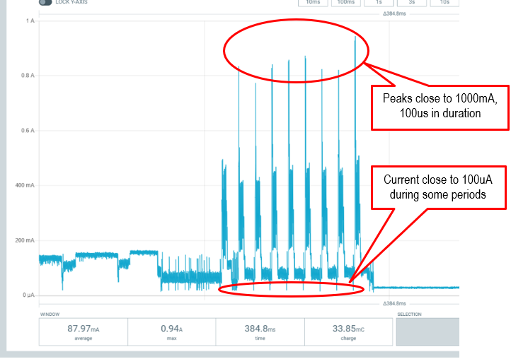
The VBAT current can vary several orders of magnitude depending on power state (as presented in Power Management). The picture below illustrates how the 1ZM M.2 current draw looks like after firmware download when internal RF calibration operations are performed. The current peaks are close to 1000mA and very narrow in time. Not all M.2 modules behaves like this, but to design a general M.2 interface that work with a wide range of M.2 modules, the VBAT power supply must be able to handle such peaks.

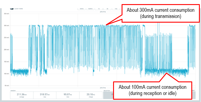
During normal Wi-Fi transmission in connected mode, especially at high RF power levels, the current consumption also varies quickly. The picture below illustrates the 1ZM M.2 module, transmitting at 177Mbps on the 5 GHz band. Current consumption switches quickly between 300mA and 100mA.

The datasheet for the used M.2 module lists the maximum current consumption. The datasheet for the corresponding Murata Wi-Fi/BT module also contains this information. Add a sufficient margin to this. 20-30% is recommended.
To support a wide range of M.2 modules including 2x2 MIMO modules, VBAT should be able to supply at least 3000mA current.
Measure the current transient response on the power supply to make sure it is stable and there are no voltage dips or peaks related to fast current changes. When you measure, be very careful to not introduce large voltage drops over a current sense resistor that is mounted in series with the VBAT power supply. Ideally, limit the voltage drop to 100mV in order not to degrade RF performance.
VBAT Low-Noise
The VBAT power supply must be low-noise because the RF performance can be severely negatively affected if there is too much noise on the VBAT supply voltage.
The allowed peak to peak ripple voltage on VBAT depends on the frequency of the noise. The higher the frequency, the lower the tolerated noise is.
Allowed ripple on VBAT is 50mV peak to peak in the 10 - 100kHz frequency range.
Allowed ripple on VBAT is 25mV peak to peak in the 100kHz - 1MHz frequency range.
Allowed ripple on VBAT is 10mV peak to peak in the >1MHz frequency range.
VBAT Power Supply Design
The power supply design for VBAT can either be a linear (likely low drop out, LDO) regulator or a switching mode power supply (SMPS).
A linear power supply design is preferred over an SMPS since it typically has much lower peak to peak ripple voltage, i.e., lower noise levels. It is however not always possible for power efficiency reasons. If, for example, a 12V supply voltage must be converted to VBAT (3.3V) the power dissipation simply is too high. An SMPS solution must be used.
The VBAT power supply must be able to provide the voltage within the specified operating range and be capable of delivering the peak current. Be careful with filters in front of the power supply (between the power supply and the M.2 connector) since filers can greatly lower the step response to current changes, i.e., to current spikes.
Note that different control loop strategies of an SMPS can generate different amount of noise (i.e., voltage variations). Fixed Pulse Width Modulation (PWM) is preferred over Pule Frequency Modulation (PFM) since PFM typically exhibits higher voltage noise levels. Some SMPS controllers use PWM control during high current loads and activate PFM control during low current load conditions. For any SMPS design, verify that the design meets all requirements on voltage stability and noise levels under all current load conditions.
VBAT Rise Time
Design the power supply so that VBAT does not rise (10 - 90%) faster than 40 microseconds and not slower than 100 milliseconds. Some Wi-Fi/BT chipsets have requirements that fall within this range.
Also make sure there is a discharge function of the VBAT supply when it is not enabled. VBAT should not exceed 200mV when not enabled. This is to ensure proper power cycles.
VBAT Operating Point
The recommended VBAT voltage is 3.3V ±5%, instead of the more normal ±10%. The reason for the recommended ±5% tolerance is that the lower value of this is often also the lower value for the Wi-Fi/BT module’s RF specification. Having a power supply with ±10% accuracy can result in operating the module outside of the M.2 module’s specification.
It is also possible to select a slightly higher operating point, say 3.4-3.5V. Note that 3.6V is maximum voltage even though the Wi-Fi/BT module accept higher VBAT voltage, other components on the M.2 module limit the maximum voltage to 3.6V.